Showing posts with label music. Show all posts

Friday, 6 December 2019

Qualcomm Windows on Snapdragon: New 7c & 8c SoCs for sub-$800 Laptops

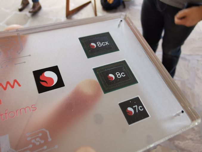
Last year Qualcomm introduced its flagship Snapdragon 8cx platform for premium always-connected PCs (ACPCs) that packed the best technologies that the company had to offer at the time. Being a no-compromise solution, the Snapdragon 8cx was not meant for every ACPC out there, so this week the company expanded the lineup of its SoCs for laptops with the Snapdragon 7c for entry-level machines and the Snapdragon 8c for mainstream always-connected notebooks.

Qualcomm aimed its Snapdragon 8cx primarily at flagship devices ACPCs and therefore maxed out its performance and capabilities, as well as offering the ability to add a 5G modem inside. To day the SoC has won only three designs: the Lenovo 5G laptop (which is yet to ship), the Microsoft Surface Pro X (which uses a semi-custom version called SQ1), and the Samsung Galaxy Book S — all of which are going to cost well over $1000.
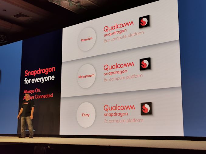
In a bid to address more affordable machines, Qualcomm will roll-out its slightly cheaper Snapdragon 8c SoC that is the same silicon as the 8cx, but will feature a tad lower performance. The 7c by comparison is a new chip that will also have a smartphone counterpart, and is aimed at sub-$400 devices, according to analyst Patrick Moorehead. Qualcomm even stated that the 7c is going to target Chromebook equivalents, if not ChromeOS itself.

Qualcomm Snapdragon Flagship SoCs 2019-2020
SoC Snapdragon 8cx Snapdragon 8c Snapdragon 7c
CPU 4x Kryo 495 Gold
4x Kryo 495 Silver
Up to 2.84 GHz
4x Kryo 490 Gold
4x Kryo 490 Silver
Up to 2.45 GHz
8x Kryo 468
Up to 2.40 GHz
GPU Adreno 680 Adreno 675 Adreno 618
DSP / NPU Hexagon 690 Hexagon 690 Hexagon ?
AI Perf Combined 7 TOPs 6 TOPs 5 TOPs
Memory
Controller
8x 16-bit CH
LPDDR4X-4266
63.58 GB/s
4x 16-bit CH
LPDDR4X-4266
31.79 GB/s
2 x 16-bit CH
LPDDR4-4266
15.90 GB/s
ISP/Camera Dual 14-bit Spectra 390 ISP
1x 32MP or 2x 16MP
14-bit Spectra 255
1x 32MP or 2x 16MP
Decode
Encode
4K120 10-bit H.265
720p480
HDR Support
4Kp60
?
HDR Support
Wi-Fi Wi-Fi 5 Wi-Fi 6
Integrated Modem Snapdragon X24 LTE
(Category 20)

DL = 2000 Mbps
7x20MHz CA, 256-QAM, 4x4

UL = 316 Mbps
3x20MHz CA, 256-QAM
Snapdragon X15 LTE
(Category 15/13)

DL: 800 Mbps
3x20MHz CA, 256-QAM, 4x4

UL: 150 Mbps
2x20MHz CA, 64-QAM
External Modem Snapdragon X55

(LTE Category 24/22)
DL = 2500 Mbps
7x20MHz CA, 1024-QAM
UL = 316 Mbps
3x20MHz CA, 256-QAM

(5G NR Sub-6 + mmWave)
DL = 7000 Mbps
UL = 3000 Mbps

-
Mfc. Process TSMC
7nm (N7)
7nm Samsung
8nm

The 8c is the same chip as the 8cx, but clocked slightly lower. The 7c by contrast is built on Samsung’s 8nm process, and will mirror the specifications of a mid-range mobile chip in 2020. We were told that the 7c chip isn’t exactly ready yet, although other press were told that demos that were supposedly on 7c devices in our briefing were actually running 7c silicon.
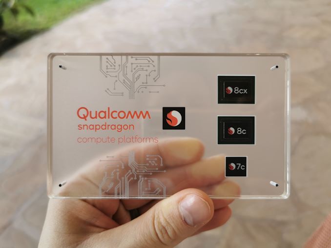
The 8c, being an 8cx variant, can be paired with Qualcomm’s X55 modem to enable 5G connectivity, although it will be up to the OEM in order to determine if the device will have both Sub 6 GHz and mmWave support.

Devices featuring the 8c and 7c should come to market in 2020.

Alex Katouzian, senior vice president and general manager of mobile at Qualcomm Technologies, said the following:

“The mobile-first consumer wants an experience on par with a smartphone, and we have the innovation, the inventions and the technology to enable this experience for customers across price points.”

Related Reading

Source: Qualcomm


from AnandTech https://ift.tt/2OXnt5S
via gqrds

Monday, 2 December 2019

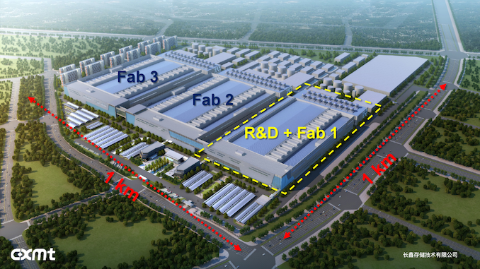
ChangXin Memory Technologies (CXMT) is Ramping up Chinese DRAM Using Qimonda IP

ChangXin Memory Technologies (CXMT), previously known as Innotron, has started production of computer memory using a 19 nm manufacturing technology. The company has a roadmap for at least two more 10 nm-class fabrication processes and plans to produce all types of DRAM in the future. Not only this, but CXMT has plans to build two additional fabs to boost its output.

Chinese authorities nowadays invest heavily in various high-tech companies as part of the country’s Made in China 2025 project. Because China consumes about a half of the global DRAM output, it makes a great sense for the government to develop the country’s own memory production industry, which is why numerous DRAM companies were established in the recent years. Innotron was among the first memory producers to be founded in 2016 and since then the company has worked hard on multiple projects.

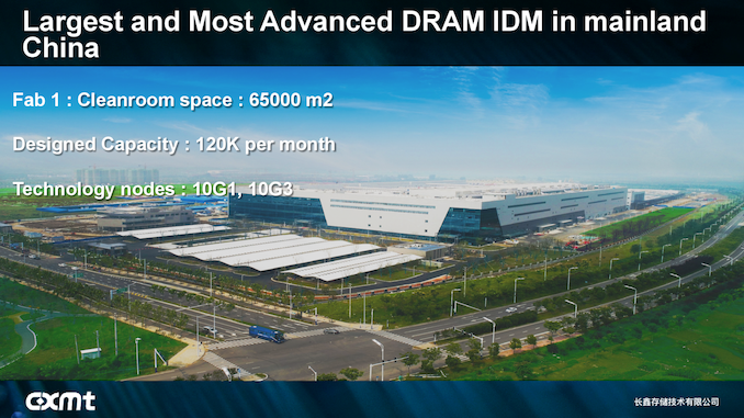
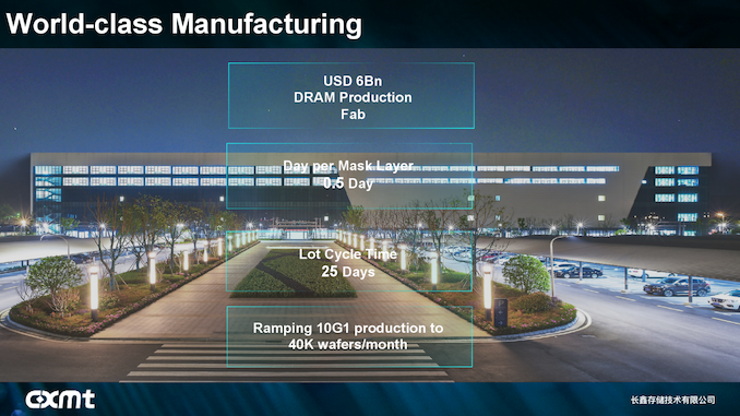
Based in Anhui, Hefei, CXMT currently has over 3,000 employees and runs a fab with a 65,000 sqare meters cleanroom space that by the end of 2020 will have 120k wafers starts (12-inch) per month using 10 nm-class process technologies (for now), which is comparable to production capacity of SK Hynix's fab in Wuxi, China. At present, the fab’s output is around 20,000 wafers starts per month, but it will increase as the company lands more orders and ramps up the fab.

According to the CXMT, 77% of its employees are engineers working on various R&D-related projects. Given recent news about certain Chinese companies potentially being involved in memory IP theft, it should be noted that CXMT has licensed IP originally designed by Qimonda. This means that it has ties with Micron, which owns that intellectual property, or just acquired it from Xi'an UniIC, which also has it. Micron's Investor Relations is involved with CXMT, so we suspect the former.

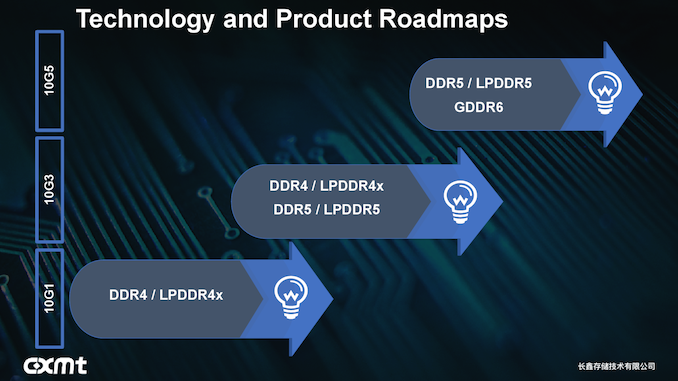
At present, CXMT uses its 10G1 process technology (aka 19 nm) to make 4 Gb and 8 Gb DDR4 memory chips with the aim to ship them commercially in Q1 2020. The same technology will be used to manufacture LPDDR4X memory in the second half of 2020. The company’s technology roadmap includes 10G3 (aka 17 nm) for DDR4, LPDDR4X, DDR5, and LPDDR5 as well as 10G5 for DDR5, LPDDR5, and GDDR6.

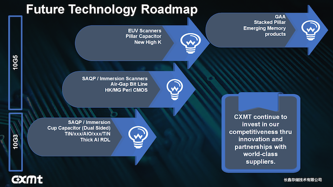
Right now, CXMT cannot rival established players either in terms of technological prowess or manufacturing capabilities. Despite this, the company is very serious about development of new fabrication processes as well as expansion of production capacities. The company’s 10G5 process will use HKMG and air-gap bit line technology, whereas technologies to be used in longer term future will use pillar capacitors, gate all-around transistors, as well as extreme ultraviolet lithography (EUVL). Not only this, but as mentioned previously, there is a plan to build two more DRAM fabs.

One thing to keep in mind about CXMT’s roadmap is that the company originally planned to start production of DDR4 memory in early 2019, but it looks like it is a year behind its original plan.

Related Reading

Source: CXMT Presentation


from AnandTech https://ift.tt/2r5g2Af
via gqrds
Friday, 29 November 2019

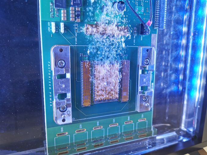
Two Phase Immersion Liquid Cooling at Supercomputing 2019

It would now appear we are saturated with two phase immersion liquid cooling (2PILC) – pun intended. One common element from the annual Supercomputing trade show, as well as the odd system at Computex and Mobile World Congress, is the push from some parts of the industry towards fully immersed systems in order to drive cooling. Last year at SC19 we saw a large number of systems featuring this technology – this year the presence was limited to a few key deployments.


from AnandTech https://ift.tt/2OBjJXv
via gqrds

Panasonic to Sell Semiconductor Business to Nuvoton

Panasonic has announced plans to almost completely withdraw from semiconductor business and sell all of its related assets to Taiwan-based Nuvoton Technology, a wholly owned subsidiary of Winbond Electronics. Under the terms of the deal, Nuvoton will get Panasonic’s semiconductor manufacturing assets, chip & product development units, contracts, and sales assets for about $250 million. Following the transaction, the only semiconductor-related property that Panasonic will have will be its 20% stake in Socionext.

Panasonic started its semiconductor business back in 1957 and was once a leading designer and maker of chips. As competition in the industry intensified early this decade, the company adopted an asset light strategy and started to gradually withdraw from both the development and manufacturing of semiconductors. In 2014, it sold a 51% stake in its chip manufacturing assets (consisting of one 300-mm and two 200-mm fabs) to TowerJazz, then Panasonic sold off its assembly/test facilities to UTAC. Finally, the company outsourced production of advanced SoCs to Intel Custom Foundry, which symbolized their withdrawal from development of leading-edge process technologies.

It did not take long for the company to realize that the design of complex SoCs was getting too expensive, which is why in March of 2015 it transferred its SoC development assets to Socionext, a joint venture between the Development Bank of Japan, Fujitsu, and Panasonic. Recently, Panasonic sold its diode and transistor business to Rohm Semiconductor. All told, Panasonic's chip business has been on a downward spiral for quite a while now.

By contrast, Nuvoton, which was established in 2008 by Winbond to produce microcontrollers, power management ICs, and other similar devices, has been quite a success. It has numerous clients and it looks like its 200-mm fab is not enough for the company. Under the terms of the agreement with Panasonic and TowerJazz, through acquisition of Panasonic Semiconductor Solutions Co. (PSCS) it will get all three Japanese fabs which originally belonged to Panasonic. Meanwhile, the sum that Nuvoton will pay to TowerJass is unknown.

Furthermore, Nuvoton will get Panasonic’s business and R&D operations related to power-management ICs, sensors (for smartphones, vehicles, and various types of cameras) and other types of products by taking over Panasonic Industrial Devices Systems & Technology (PIDST), Panasonic Industrial Devices Engineering (PIDE), and Panasonic Semiconductor Suzhou (PSCSZ) companies.

As a result of the business transaction, Nuvoton will own four semiconductor manufacturing facilities: one 300-mm fab and three 200-mm fabs. Moreover, it will get a rich portfolio of products, customers, and contracts. However it will also be inheriting the debts of the aforementioned companies. Ultimately this will allow Panasonic to exit the semiconductor business, improving its own financial position.

Related Reading:

Sources: Panasonic, Nuvoton. Taipei Times, Reuters


from AnandTech https://ift.tt/33sF09L
via gqrds
Monday, 11 November 2019

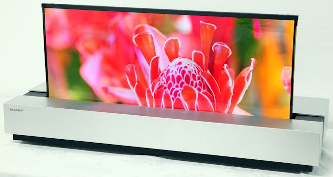
Sharp & NHK Develop Rollable 30-Inch 4Kp60 OLED Screen: 100 Grams and 0.5 mm Thick

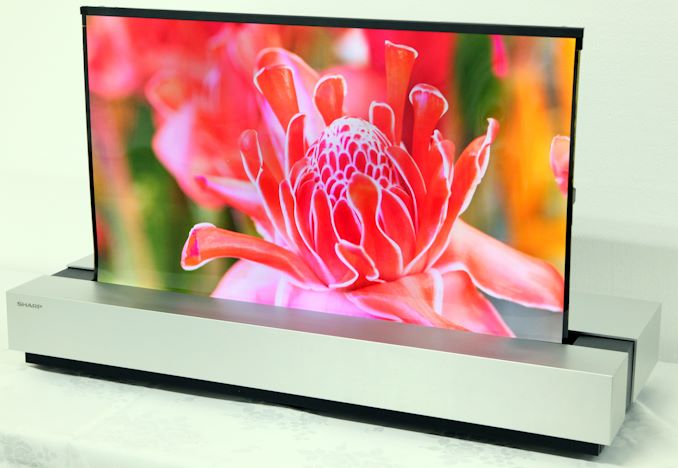
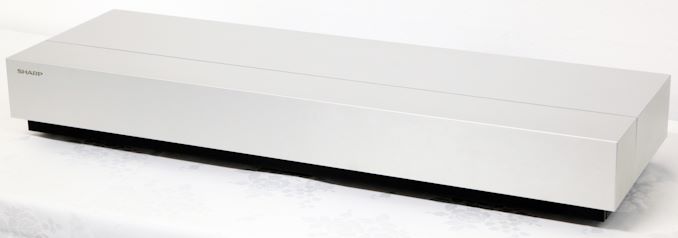
Sharp and NHK have co-developed a new rollable 30-inch OLED display, with a design emphasis on keeping the screen thin and light. The prototype monitor will be showcased at a trade show in mid-November, but the company isn't yet talking about mass production.

The experimental 30-inch OLED display offers a 3840×2160 resolution and a 60 Hz refresh rate, all in a package that is just 0.5 mm thick and weighs 100 grams. The developers say that the screen can be rolled up into a 4 cm diameter cylinder, with the idea of being able to integrate the display into various appliances like furniture. Meanwhile, the technology itself could simplify production of foldable electronics, such as smartphones and tablets.

The flexible 30-inch OLED display is produced by Sharp at one of its factories in Japan using vapor deposition method. The screen uses a film substrate and IGZO thin film transistors to drive OLED elements that use separate RGB subpixels. Meanwhile, NHK’s image processing technologies were used to improve brightness uniformity as well as sharpness of moving objects.

Sharp and NHK will demonstrate their prototype rollable 30-inch OLED display at Intel's BEE 2019 trade show, which will take place in Chiba, Japan, from November 13 to November 15.

Sharp and NHK are not the only companies to develop a rollable OLED screen. Earlier this year LG demonstrated such a TV at CES 2019 and even started to sell its rollable Signature TVs in South Korea.

Related Reading:

Sources of information and images: Sharp, CNET Japan, PC Watch, StereoSoundOnline


from AnandTech https://ift.tt/36MZ21E
via gqrds
Microsoft’s HoloLens 2 Now Available for $3,500

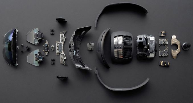
Microsoft has started sales of its HoloLens 2 mixed reality smart glasses. Aiming to be a significant upgrade over its predecessor in both field and overall performance, the second generation of the company's head-mounted computer is geared primarily towards enterprise organizations, where Microsoft and its partners are continuing to experiment with and develop practical applications for augmented reality in the workplace.

From a tech perspective, Microsoft’s HoloLens 2 isn't a radical departure from the original HoloLens in terms of features and basic design goals, but as a second-generation product Microsoft has put a lot of work into improving the technology and the user experience. HoloLens 2's visual system offers a 52º diagonal field-of-view (up from 34º) with a resolution of 47 pixels per degree on its MEMS display. Under the hood, it is based on Qualcomm’s Snapdragon 850 as well as Microsoft’s custom holographic processing unit (HPU) 2.0 chips, which should offer a drastically higher performance than the previous-generation hardware. Finally, the product features better ergonomics and revamped interaction model with full-blown hand tracking and improved visuals.

As noted above, the HoloLens 2 is still focused primarily on businesses and organizations that can take advantage of the device in their workflows. Microsoft will continue to support the original HoloLens, but customers can now deploy the improved version.

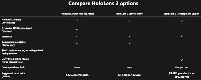
Microsoft offers three options to buy its HoloLens 2. The a stand-alone HoloLens 2 device with Windows 10 Holographic is available from select resellers for $3,500. The HoloLens Development Edition with Windows 10 Holographic, a $500 credit for Azure (including mixed reality services), and Unity Pro & PiXYZ Plugins (with a three-months license) pre-installed can be purchased for $3,500 (or $99 per month). Finally, there is HoloLens 2 with Remote Assist version for enterprises that comes with Windows 10 Holographic and Dynamics 365 Remote Assist that can be had for $125 per user per month.

Related Reading:

Sources: Microsoft


from AnandTech https://ift.tt/2p6MvoL
via gqrds
Friday, 8 November 2019

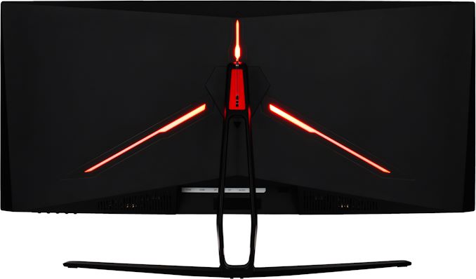
Nixeus Launches NX-EDG34: A Curved 34-Inch WQHD Monitor w/ 144 Hz & FreeSync

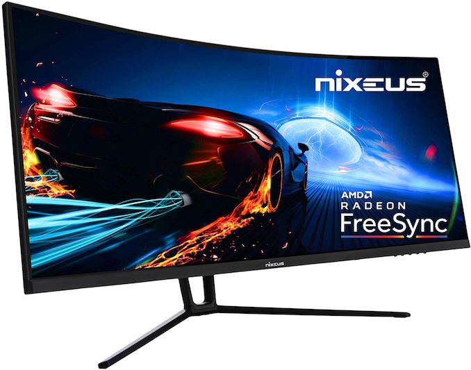
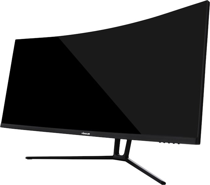
Nixeus this week took the wraps off its latest curved ultrawide NX-EDG34 gaming display, which blends together a large size, a WQHD resolution, a 144 Hz maximum refresh rate, and AMD’s FreeSync dynamic refresh rate technology. At present, only a few monitors can boast the same combination of features that the EDG34 has to offer, so it will be in a rather unique position when it becomes available.

The Nixeus NX-EDG34 display builds upon a curved VA panel with a 3440×1440 resolution, and is capable of reaching 350 nits typical brightness (400 nits in HDR mode), a 3000:1 contrast ratio, a 21:9 aspect ratio, 178°/178° viewing angles, and a 4 ms GtG response time. In terms of refresh rates, the monitor's maximum rate is 144 Hz, and in variable refresh mode it operates in a 48 Hz – 144 Hz range. The LCD can display 16.7 million colors and supports an HDR mode, which suggests a wider-than-sRGB color gamut.

Because the Nixeus NX-EDG34 is designed for gamers, it naturally features multiple inputs to connect a PC (or two) and a couple of game consoles, so it has two DisplayPorts 1.4 and two HDMI 2.0 ports. It is also equipped with a headphone jack.

From design standpoint, the Nixeus NX-EDG34 has very thin bezels on three sides as well as red LEDs on the backside to emphasize gaming nature of the device. Nixeus will offer two versions of its new monitor: the NX-EDG34S with a stand that can adjust tilt as well as the NX-EDG34 that can adjust both tilt and height.

Nixeus NX-EDG34 Displays
  NX-EDG34
NX-EDG34S
Panel 34" VA
Native Resolution 3440 × 1440
Brightness 350 cd/m² typical
400 cd/m² HDR
Contrast 300:1
Maximum Refresh Rate 144 Hz
Variable Refresh Rate AMD FreeSync
48 Hz ~ 144 Hz
Response Time 4 ms GtG
Viewing Angles 178°/178° horizontal/vertical
Curvature 1500R
Pixel Pitch 0.233 mm
Pixel Density 110 ppi
Anti-Glare Coating ?
Inputs 2 × DisplayPort
2 × HDMI 2.0
USB Hub No
Stand NX-EDG34: height and tilt adjustable
NX-EDG34S: tilt adjustable
75x75 VESA mount
Audio headphone output
Launch Price $500 ~ $550

Nixeus will start shipments of its NX-EDG34S display in late November or early December, depending on the retailer. At present, the monitor can be pre-ordered for $499.99 from Newegg or for $551.15 from Amazon.

As an aside, while 34-inch ultrawide WQHD displays are gaining traction, there are just a few gaming monitors from popular brands that feature a 3440×1440 resolution with high refresh rate (i.e., 100 and higher). In fact, the only product that has the same specs as the EDG 34 is Xiaomi’s Mi Surface Display that was introduced back in October, but that is only available in China (and we do not know if and when it will be sold in other countries). Another, similar monitor is MSI’s Optix MAG341CQ, that has just a 100 Hz refresh rate and is priced at $428.99. Finally, there is Dell’s latest Alienware 34 LCD with as an IPS panel and a 120 Hz refresh rate, but it is priced at a whopping $1499.99. All things considered, the Nixeus NX-EDG34 will be in a unique position in the US at least for a while before other makers adopt the same LCD panel.

Related Reading:

Source: Nixeus


from AnandTech https://ift.tt/33tO4Mp
via gqrds
Thursday, 7 November 2019

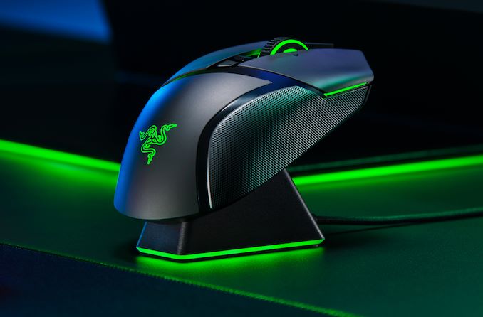
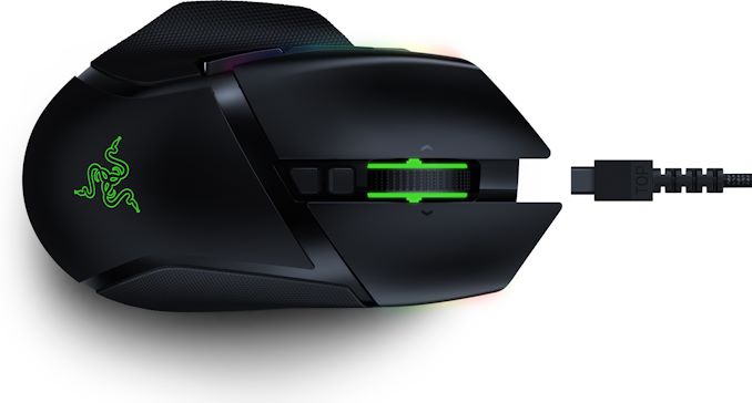
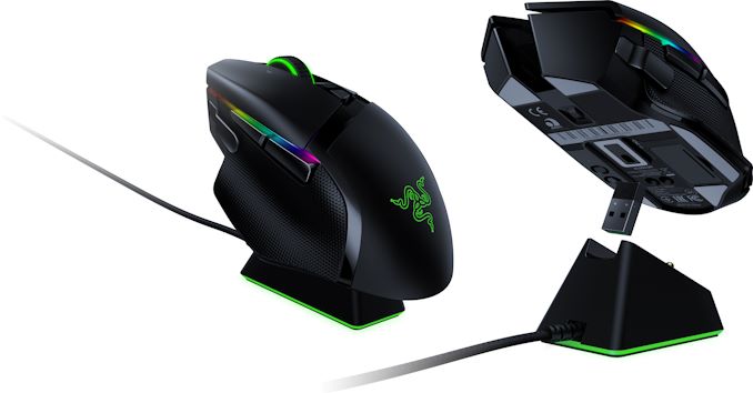
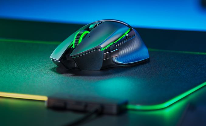
Razer Unveils Basilisk Ultimate Wireless Mouse: 20,000 DPI & Low Lag

Razer has announced its new flagship Basilisk Ultimate wireless gaming mouse aimed at esports and FPS gamers. The Basilisk Ultimate uses Razer’s latest sensor, latest optical switches, and features a HyperSpeed wireless connectivity technology that promises an ultra-low lag. To make the mouse catch eyes, it features 14 RGB lighting zones that can be programmed using the company’s software.

The Razer Basilisk Ultimate is based on the company’s in-house designed Focus+ optical sensor featuring a 20,000 SPI precision, a 650 IPS maximum speed, and a 50G acceleration. The sensor is paired with an SoC that enables multiple features which improve its accuracy and cut down response time of this wireless mouse. In particular, the Smart Tracking capability automatically calibrates the sensor across different surfaces; the Motion Sync aligns polling rates of the host PC, receiver, and sensor to reduce input lag; whereas the Asymmetric Cut-off further improves precision by setting an accurate lift-off distance.

Besides the proprietary Focus+ sensor, the Razer Basilisk Ultimate also uses the company’s own HyperSpeed wireless technology that uses a 4 GHz band and a special dongle as well as features the Adaptive Frequency Hopping that scans interconnection channels and switches to the one with the lowest interferences to ensure the lowest lag. Meanwhile, it is possible that HyperSpeed also optimizes lag on the software side of things, though Razer does not talk about it.

When it comes to ergonomics, the Basilisk Ultimate is a right-handed mouse with a scrolling wheel as well as 11 programmable controls (onboard or cloud storage). Sensitivity of the device can be adjusted on the fly using a special paddle on the left side of the unit, a common feature on contemporary gaming mice.

Razer’s Basilisk Ultimate will be available directly from the company as well as from its retain partners starting from November 6. The mouse itself will cost $149.99/€169.99, the mouse with its dock will be priced at $169.99/€189.99, whereas the dock sold separately will carry a $49.99/€59.99 price tag. Without the dock, the Basilisk Ultimate can be charged using a micro-USB cable that also enables the mouse’s wireless mode for the lowest lag possible.

Related Reading

Source: Razer


from AnandTech https://ift.tt/2qsEFpT
via gqrds

Tuesday, 5 November 2019

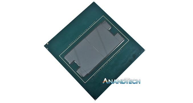
Intel’s EMIB Now Between Two High TDP Die: The New Stratix 10 GX 10M FPGA

The best thing about manufacturing Field Programmable Gate Arrays (FPGAs) is that you can make the silicon very big. The nature of the repeatable unit design can absorb issues with a process technology, and as a result we often see FPGAs be the largest silicon dies that enter the market for a given manufacturing process. When you get to the limit of how big you can make a piece of silicon (known as the reticle limit), the only way to get bigger is to connect that silicon together. Today Intel is announcing its latest ‘large’ FPGA, and it comes with a pretty big milestone with its connectivity technology.


from AnandTech https://ift.tt/32iGT8v
via gqrds
Friday, 1 November 2019

Rambus Demonstrates GDDR6 Running At 18 Gbps

While GDDR6 is currently available at speeds up to 14Gbps, and 16Gbps speeds are right around the corner, if the standard is going to have as long a lifespan as GDDR5, then it can't stop there. To that end, Rambus this week demonstrated operation of its GDDR6 memory subsystem at a data transfer rate of 18 GigaTransfers/second, a new record for the company. Rambus’s controller and PHY can deliver a peak bandwidth of 72 GB/s from a single 32-bit GDDR6 DRAM chip, or a whopping 576 GB/s from a 256-bit memory subsystem, which is what we're commonly seeing on graphics cards today.
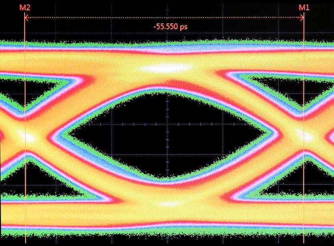
The Rambus demonstration involved the company’s silicon-proven GDDR6 PHY implemented using one of TSMC’s 7 nm process nodes, accompanied by Northwest Logic’s GDDR6 memory controller and GDDR6 chips from an unknown maker. According to a transmit eye screenshot published by Rambus, the subsystem worked fine and the signals were clean.

Both GDDR6 controller and PHY can be licensed from Rambus by developers of SoCs, so the demonstration is both a testament to how well the company’s highly-integrated 7 nm GDDR6 solution works, and a means to promote their IP offerings.

It is noteworthy that Rambus, along with Micron and a number of other companies, has been encouraging the use of GDDR6 memory in products besides GPUs for quite some time. Various accelerators for AI, ML, and HPC workloads as well as networking gear and autonomous driving systems greatly benefit from the technology's high memory bandwidth and are therefore a natural fit for GDDR6. The demonstration is meant to show companies developing SoCs that Rambus has a fine GDDR6 memory solution implemented using a leading-edge process technology that can be easily integrated (with the help of engineers from Rambus) into their designs.

For the graphics crowd, Rambus’ demonstration gives a hint of what to expect from upcoming implementations of GDDR6 memory subsystems and indicates that GDDR6 still has some additional room for growth in terms of data transfer rates.

Related Reading:

Source: Rambus


from AnandTech https://ift.tt/36oIUmW
via gqrds

Sony to Build New Fab to Boost CMOS Sensor Output

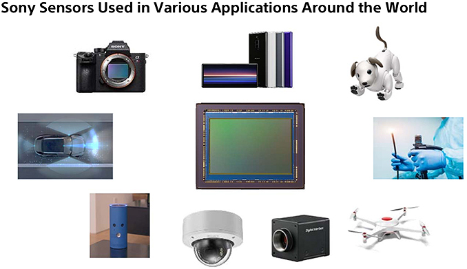
Sony this week has revealed that the company will be building a new semiconductor fab to boost output of its CMOS sensors, as part of a broader effort to respond to growing demand for these products. The company will build the new fab at its Nagasaki Technology Center and expects it to tangibly increase their production of CMOS wafers.

Being one of the leading suppliers of CMOS camera sensors for smartphones, Sony earns billions of dollars selling them. In the third quarter (Q2 FY2019) Sony’s Imaging and Sensing Solutions (I&SS) division earned $2.871 billion in revenue (up 56.3% year-over-year) and $706 million in profits*. As of late March 2018, Sony’s CMOS production capacity was 100 thousand 300-mm wafer starts per month, and the company is gradually increasing its output by improving efficiency of its fab space utilization and outsourcing part of the production. But that may not be enough.

In the coming years demand for CMOS sensors is going to grow because of several factors: smartphones now use not two (for main and selfie cameras), but three or even more camera modules; smartphone sensors are getting larger; and more devices are going to get computer vision support, requiring more sensors there as well.

In order to satisfy demand for such products, the company constantly improves its fabs and expects to boost their total output capacity to around 138 thousand of wafer starts per month by late March 2021. Furthermore, Sony plans to invest billions of dollars (PDF, page 152) in fab upgrades as well as building an additional fab (or even fabs) at its Nagasaki Technology Center. The new manufacturing facility (or facilities) is expected to start production sometime during the company's 2021 fiscal year, which starts on April 1, 2021. That being said, it is reasonable to expect that Sony is aiming to start construction of the facility in the coming months.

It is noteworthy that Sony’s semiconductor division (which is now called I&SS) reportedly has not invested anything in brand-new production facilities for 12 years. The company did acquire a semiconductor fab from Toshiba and then re-purposed it to make sensors in 2016, but this was not a new fab. Apparently, Sony now forecasts such high demand for sensors in the coming years that it has decided to invest in all-new production lines.

Sony’s statement reads as follows:

“We expect demand for our image sensors to continue to increase from next fiscal year as well due to the adoption of multi-sensor cameras and larger- sized sensors by smartphone makers.

In order to respond to this strong demand, we have further improved the efficiency of space utilization in our existing factories and have raised our production capacity target for the end of March 2021 from 130,000 wafers per month to 138,000 wafers per month.

Moreover, we have decided to move forward in stages with the investment we had been considering to build new fabs at our Nagasaki facility to accommodate demand from the fiscal year beginning April 1, 2021.

Through this action, we are working to continue growing the I&SS business so as to achieve the mid-range targets we established at the IR Day this year: 60% revenue share of the image sensor market and 20-25% ROIC in the fiscal year ending March 31, 2026.”

*For the sake of clarity, it is necessary to note that Sony’s I&SS division still produces some chips for Sony’s needs, so not 100% of its revenue comes from image sensors

Related Reading:

Sources: Sony, Sony, Nikkei, ElectronicsWeekly, Reuters


from AnandTech https://ift.tt/2N8o83j
via gqrds